Vertical MOSFETs for RF application
Over the past 20 years, the channel length of MOS transistors has halved roughly every 3 years. This has led to increasingly complex CMOS electronic circuits operating at higher clocking cycles and decreasing cost.
Professor S Hall and Dr I Mitrovic
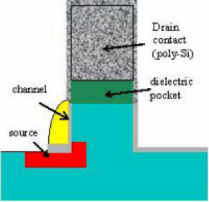
A number of factors pose a threat to the evolution of CMOS technology, the most significant of which is the difficulty of defining the transistor dimensions with conventional optical lithographic tools. One remedy is to use new tools but this may be prohibitively expensive. An alternative strategy is to exploit the excellent control of thin layers achievable by epitaxial growth and dopant ion-implantation to produce very short channel vertical rather than conventional lateral transistors. This should allow channel lengths down to 0.02 mm with conventional lithographic tools. A SiGe layer can be incorporated into the source region to reduce parasitic bipolar effects. Figure 1 below shows a device concept under consideration. The device incorporates a retrograde channel realised by epitaxial growth over the vertical turret. A dielectric ‘pocket’ on top of the turret helps to suppress short channel effects. This architecture should allow scaling to 50nm channel length.
The project is concerned with modelling of such device structures to gain insight into the operation and design of MOSFETs realised this way together with the development of new processing schedules to allow practical realisation of the transistors. A crucial aspect is the realisation of very thin gate oxide (~2nm) on a vertical sidewall and a number of advanced oxide assessment techniques will be established to allow its detailed characterisation. The transistors are to be incorporated into analogue circuit building blocks: low noise amplifier, power amplifier, local oscillator etc.  Figure 1 - Vertical MOS concept