Plasma oxidation of silicon and silicon-geranium
Current research is conducted through the technology strategy board project PPM2 in collaboration with PlusSemi, TWI, Qudos and JLS. The aim is to produce high precision capacitors for use in application areas such as radio-frequency, energy harvesting, medical and low power.
Professor S Hall and Professor S Taylor
Plasma oxidation involves the growth rather than deposition of high quality thin layers of silicon oxide at room temperature. The technique employs O- produced in oxygen plasma. It is a technique that has been pioneered in the department. Because of the low growth temperature, it has been effective as the gate dielectric for polysilicon thin film transistors produced on low cost, low melting point, display glass; for advanced structures, employing delta-doped layers where no thermal induced diffusion can be allowed and in the definition of 15nm lines in silicon oxide as part of the process of developing ultra small channel length MOS devices. It is the only low temperature technique capable of producing high quality layers and interfaces on SiGe alloys.
Figure 1 - Typical source-drain characteristics of the first boron delta doped field-effect transistor. Gate oxide fabrication in this Department.
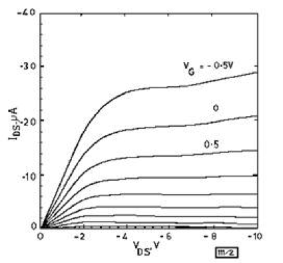
Figure 2 below shows SiGe MOST device structures featuring surface channels formed in an epitaxial SiGe material. The gate oxide is grown by plasma oxidation. The SiGe channel causes enhancement of hole mobility.
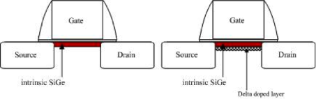
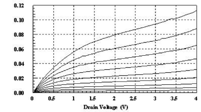
Figure 3 - Experimental output characteristics of 0.1mm SiGe channel MOSFET