More Moore
"More Moore": the limits of micro- and nanolithography
This set of research projects will look, both from an experimental and simulation point of view, at the limits of nano-fabrication and nano-manipulation of nano-objects.
The proposed experimental stream of sub-projects will study, for instance:
- Fabrication of polymeric nanostructures using atomic force microscopy (AFM)
- Resilience of polymeric nanofabricated structures versus molecular relaxation phenomena
- Manipulation of nanoobjects (eg. metallic beads) using AFM, in particular in micro/nano-fabricated structures
- Fabrication of 3D sub-micrometer structures using larger size microlithography techniques, eg. laser microablation of nanometer thick metallic layers deposited on polymers, etc.
The modelling and simulation stream of projects will study, for instance:
- Process latitude of microlithography in classical mode and using novel manipulation of light (eg. built in molecular masks)
- Result of the impact of nano-objects (eg. fullerenes) on semiconductor, metallic and polymeric materials.
Both these lines of projects are of extreme and acute importance to the present semiconductor industry, and hence will better position the students interested to pursue a career in this area with a strong industrial/applied research character.
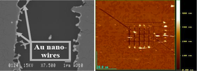
Figure 1 below show gold nanowires fabricated through the microablation of nanometre thick Au layers on polymers (left), and 20 to several hundred nm nanostructures fabricated with atomic force microscope.