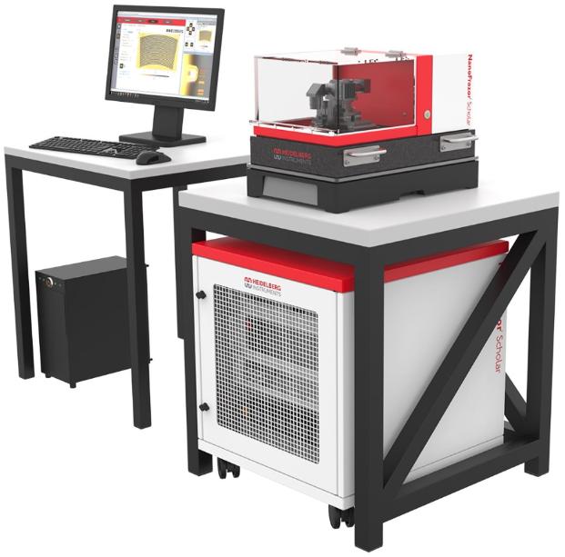
Nanolithography suite
The Heidelberg Instrument NanoFrazor Scholar is a thermal scanning probe lithography system capable of 20 nm resolution nanopatterning of thin films and substrates.
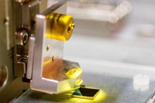
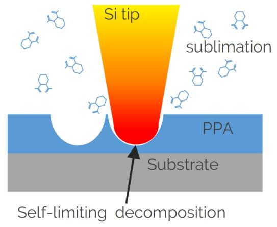
Thermal scanning probe lithography is a technology that uses an ultra-sharp heated probe tip to simultaneously write and image nanostructures. The heated tip creates arbitrary, high-resolution nanostructures by local sublimation of resists. Standard pattern transfer methods like lift-off or etching can then be applied to pattern a thin film or substrate of interest.
To pattern a complex geometry at the nanoscale, the sample is coated in a thermally sensitive polymer layer, known as a resist. PPA is typically used as a resist layer for the NanoFrazor system. The PPA resist decomposes upon heating by the tip into volatile molecules. The decomposition of the PPA is endothermic, minimising spread of heat throughout the rest of the sample.
The tip is scanned across the surface of the substrate, heating selected areas and decomposing the resist into the designed pattern. A feedback algorithm allows the depth of patterning to be constantly monitored, allowing for depth-resolved patterning into the resist.
Using wet chemical etching a sacrificial polymer layer can then be removed, exposing areas of the sample. Standard pattern transfer, including metallisation via physical vapour deposition or dry etching can then transfer the written pattern into the material of choice.
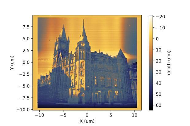
The core equipment within this research facility allows users to write complex 2D or multi-level 3D patterns onto a sample of interest, down to ~10 nm resolution, and can provide pattern transfer to, e.g., polymers, 2D materials, metals, semiconductor heterostructures, and oxide thin films.
The suite has combined tools with basic ancillary resist developing/processing (including spin coating, plasma ashing and physical vapour deposition) along with a combined ball and wedge wirebonder (F&S Bondtec 53xxBDA), for electrically contacting small areal footprint samples, to ensure a complete process for most common applications.
Advantages of thermal scanning probe lithography are fast patterning, no radiation/charged particle damage, real-time imaging of patterned device, no proximity correction needed during patterning.
The tool is available to UoL researchers, as well as external industry and academic users. Access for external users will be charged - please contact the facility to discuss requirements.
Contact info
Tool capabilities
|
Writing performance |
|
| Minimum structure size [nm] | 20 |
| Minimum lines and spaces [half pitch, nm] | 30 |
| Grayscale / 3D-resolution (step size in PPA) [nm] | 3 |
| Writing field size [X μm x Y μm] | 50x50 |
| Field stitching accuracy [nm] | 50 |
| Overlay accuracy [nm] | 50 |
| Write speed (typical scan speed) [mm/s] | 0.5 |
| Write speed (50 nm pixel) [μm2/min] | 500 |
|
AFM imaging performance |
|
| Lateral imaging resolution (feature size) [nm] | 10 |
| Vertical resolution (topography sensitivity) [nm] | 0.2 |
| Imaging speed (@ 50 nm resolution) [μm2/min] | 500 |
|
System features |
|
| Substrate sizes | 1 x 1 mm2 to 50 x 50 mm2, 0 – 20 mm thickness |
| Optical microscope | 3.6 μm optical resolution, 1.5 mm x 1.1 mm field of view |
| Magnetic cantilever holder | Fast (< 1 min) and accurate tip exchange |