Facilities

Our state-of-the-art electron microscopy facilities offer cutting edge technology and expertise in a wide range of SEM analytical techniques, working through a whole range of scales, from sub-micron to centimetre in size.

Our expertise in electron backscatter diffraction (EBSD) is at the forefront of our research, and all our scanning electron microscopes (SEMs) are attached with Oxford Instruments' energy dispersive X-ray spectroscopy (EDS) detectors to provide in-depth compositional analysis.

We also specialise in a range of sample preparation methods and sample coating techniques. More details and technical specifications of our microscopes can be found below.
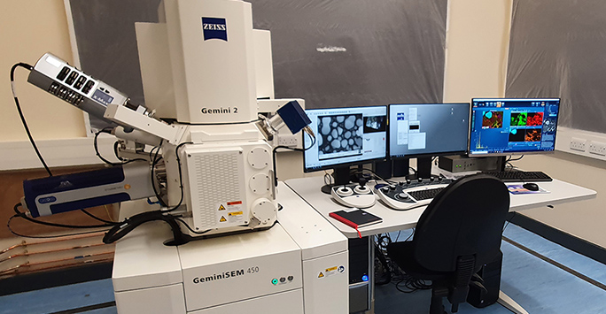
Zeiss SEM Zeiss GeminiSEM 450

Zeiss GeminiSEM 450

An ultra-high-resolution FEG SEM with variable pressure (VP) system, optimised for simultaneous electron backscatter diffraction (EBSD) and energy dispersive X-ray spectroscopy (EDS). Equipped with Oxford Symmetry EBSD and X-Max EDS detectors, and DEBEN panchromatic CL detector.

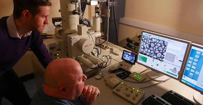
JEOL JSM 7001F FEG-SEM JEOL JSM 7001F FEG-SEM

JEOL JSM 7001F FEG-SEM

Utilises an in-lens Schottky field emission source and offers a resolution down to 1.2 nm at 30 kV. Equipped with retractable BSE detector, and Oxford Ultim-Max EDS detector with AZtec Live

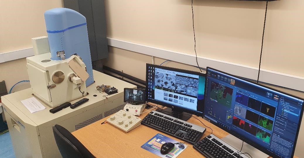
JEOL JSM 6610 SEM

JEOL JSM 6610 SEM

Utilises a thermionic tungsten (W) filament up to 30 kV offering a resolution down to 3.0 nm. Equipped with Oxford Xplore EDS detector with AZtec Live.

Electron backscatter diffraction (EBSD) Electron backscatter diffraction of gold

Electron backscatter diffraction (EBSD) in the scanning electron microscope (SEM)

A high-resolution, high-speed technique which enables the mapping of crystallographic orientations in any crystalline material.

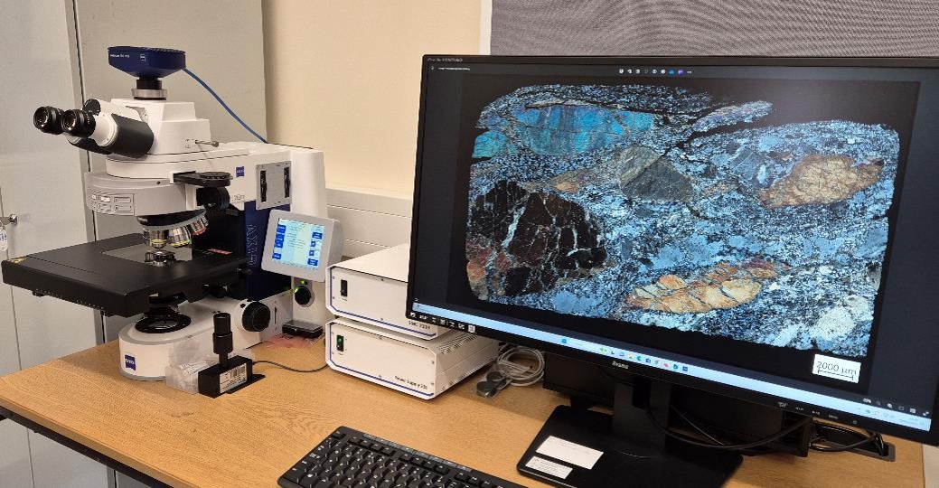
Zeiss Axio Imager 2

Zeiss Axio Imager 2

A powerful optical microscope designed specifically for materials research, large area mapping and correlative microscopy.