Engineering
Our research in engineering materials focuses on understanding material properties and performance. We use electron microscopy to examine the fine details of materials used in fields including additive manufacturing, nuclear engineering and materials for aerospace. This critical analysis informs the design of safer, more durable parts for a wide range of applications, from jet engines to medical implants.
Advanced Manufacturing
Research performed by Alfred Sidambe (et al) demonstrates that pure tantalum, a high-cost refractory metal used in biomedical and electronic applications, can be successfully processed using high-productivity Laser Powder Bed Fusion (LPBF) at a relatively low energy density. Electron Backscatter Diffraction (EBSD) analysis revealed that this process produces an anisotropic grain structure with elongated columnar grains showing a strong <111> preferential growth direction, which differs from the standard <100> orientation found in conventional tantalum.
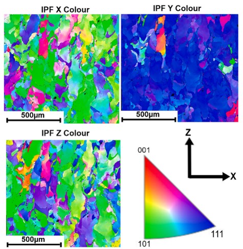
Figure: Inverse Pole Figures (IPFs) of the build direction (x-z) view of LPBF tantalum specimens.
Sidambe, A. T., Bilton, M., Black, K., & Fox, P. (2025). Densification, microstructure, crystallographic texture and mechanical properties in increased productivity laser additive manufacturing of pure tantalum. International Journal of Refractory Metals and Hard Materials, 133, 107339. doi:10.1016/j.ijrmhm.2025.107339
Laser Diagnostics
Research by Tong Zhou and the Laser Group at Liverpool explores the ultrafast laser ablation of stainless steel, copper, and silicon to study the interaction of coalescing shock waves in ambient gases. By using multi-spot patterns, the study reveals that supersonic Mach shocks accelerate nanoparticle debris into highly symmetric "jets" and "filaments" that mirror the laser’s geometry.
Scanning Electron Microscopy (SEM) of these complex redeposition patterns and, when combined with EDX, confirmed that the resulting debris consists of oxidised, agglomerated nanoparticles. These findings offer a new, small-scale diagnostic window for understanding blast wave interactions applicable to both industrial laser cleaning and structural resilience against large-scale explosions.
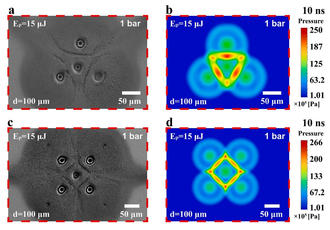 Figure: SEM images of the multi-spot HE p = 15 μ J, debris field observed during ablation on stainless steel in air and corresponding CFD simulations. a 3 + 1 spot ablation showing debris removal. b simulation of corresponding HE P around the centre with similar dimensions. c HE P , 3 + 1 pressure field at delay time Δt = 10 ns highlighting the triangular pressure field symmetry , 5 spot pattern with debris field removal in a square pattern round the centre spot. d simulation of HE pressure field at delay time Δt = 10 ns which replicates this well-defined square symmetry.
T. Zhou, S. Kraft, Z. Fang, W. Perrie, M. Bilton, J. Schille, U. Löschner, S. E. Rigby, S. Edwardson, G. Dearden (2024). Optics & Laser Technology. https://doi.org/10.1016/j.optlastec.2024.110739
Lead-free Perovskites
Research by Bei Qian (et al) demonstrates a sustainable, ambient-air fabrication strategy for lead-free double perovskite (Cs2AgBiBr6) films, which are promising non-toxic alternatives for solar cells, photodetectors, and memristors.. By utilising an ethyl acetate antisolvent treatment, the study overcomes moisture-induced defects to achieve dense, uniform films that yield a fivefold improvement in power conversion efficiency compared to untreated samples.. SEM and EDX mapping helped to confirm that this green process successfully eliminated large aggregates and substrate pinholes, resulting in a compact morphology essential for high-performance optoelectronic devices.
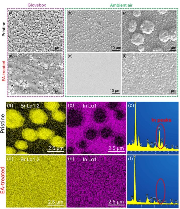
Figure: Upper - Top surface SEM images for the (a) glovebox-processed pristine films and ambient-processed pristine films under (b) low-magnification and (c) high-magnification. (d) Glovebox-processed EA-treated film and ambient-processed EA-treated films under (e) low-magnification and (f) high magnification. Lower: Top surface EDX elemental mapping of (a) Br and (b) In for the ambient-processed pristine film, (d) Br and (e) In for the ambient-processed EA-treated film. EDX spectrum for ambient-processed (c) pristine and (f) EA-treated films.
Chen, Q., Singh, A, K., Alghathami, H., Liu, X., Huang, K., Thomas, A, G., Curry, R, J., Phillips, L, J., Hughes, A, J. Green Chem., 2025. https://doi.org/10.1039/D5GC00722D