Advanced materials
Research focuses on the development, characterisation, and application of next-generation materials to address some of the world’s most pressing challenges. We collaborate across disciplines to innovate in areas such as renewable energy, sustainable technologies, and healthcare.
Biofilm Characterisation
Research From Dr. Jiaqi Luo and Prof Rasmita Raval investigated the complexities of determining the live-dead state of Staphylococcus aureus biofilms grown on silicon wafers and glass substrates using a common SYTO 9-propidium iodine (PI) staining kit. These materials serve as models for surfaces across various sectors, including medical devices (e.g., catheters and implants), food safety, and marine biofouling. High-resolution morphological data acquired by SEM revealed that a cell's physical appearance (size, shape, and membrane integrity) often does not correlate directly with the physiological state indicated by fluorescent dyes
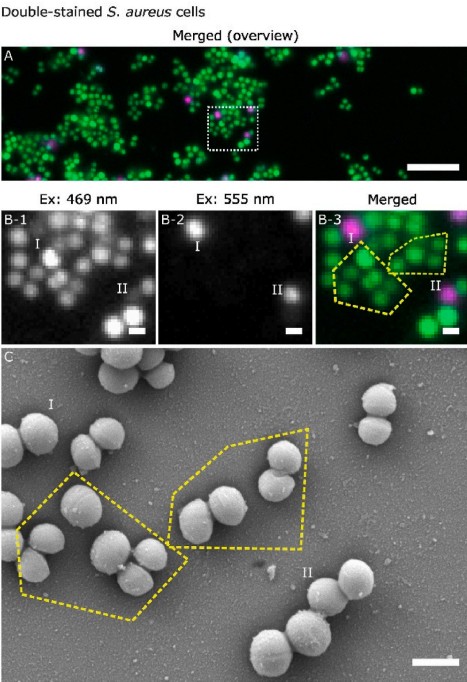
Figure: Correlative WFM-SEM data for SYTO 9 – PI stained S. aureus biofilms showing double-stained cells.
Luo, J. Raval, R. Biofilm (2025). https://doi.org/10.1016/j.bioflm.2025.100302
Nanolithography
Research by Liam Chandler (et al) in the Stephenson Institute for Renewable Energy (SIRE) outlines a methodology for fabricating artificial, nanoscale quasiperiodic tilings using thermal-scanning probe lithography (t-SPL) combined with physical vapour deposition. The study utilises permalloy (Ni80Fe20) thin films deposited onto silicon substrates to create complex patterns such as Penrose and Ammann-Beenker tilings. These fabricated structures have significant applications in engineering nanomagnetic arrays, improving solar cell efficiency, and developing photonic quasicrystals. Characterisation by SEM inspects the physical dimensions and pattern quality both before and after material deposition, as well as verifying the accuracy of the in situ thermal microscopy images.
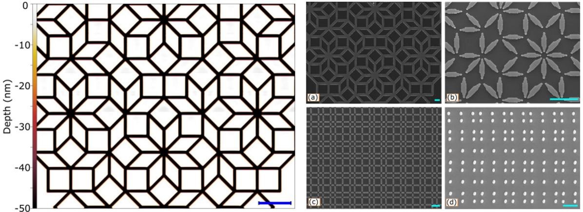
Figure: (left) A thermal-conductance microscopy image of an 8-foldAmmann-Beenker Tiling with steep edges produced in situ by t-SPL, and etched depth on the left, scale bar 5 μm. Right: SEM images of 25 nm permalloy arranged into various quasiperiodic tilings with tailored decorations. (a) Connected 8-fold Ammann-Beenker. (b) Disconnected 8-fold Ammann-Beenker 10 nm thick (c) Disconnected 4-fold Square Fibonacci tiling. (d) Vertices of the 4-fold Square Fibonacci tiling. Scale bars 1 μm.
L. Chandler, O. J. Barker, A. J. Wright, L. O'Brien, S. Coates, R. McGrath, R. Lifshitz, H. R. Sharma, Isr. J. Chem. 2023, e202300115. https://doi.org/10.1002/ijch.202300115