Transparent Semiconductor Alloy, Indium Gallium Oxide
In January, our paper titled: “Indium Gallium Oxide Alloys: Electronic Structure, Optical Gap, Surface Space Charge, and Chemical Trends within Common-Cation Semiconductors” was published in the journal ACS Applied Materials and Interfaces. This work was written by recently graduated PhD student, Dr Jack Swallow and supervised by Prof Tim Veal. Jack is now a postdoctoral researcher in the Department of Materials, University of Oxford. The work was started in the 2015 by Phil Murgatroyd when he was an undergraduate physics student in the department, as part of his research council-funded 10-week vacation research project. His initial data analysis and optical transmission spectroscopy informed the later work and the final manuscript. Phil went on to do a condensed matter physics PhD with Dr Jon Alaria and his thesis is about to be submitted.
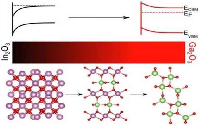
Indium oxide is ubiquitous as a transparent conductor in applications such as light emitting diodes (LEDs), thin film solar cells, flat panel displays and touch screens. For some applications, such as solar blind detectors and ultraviolet LEDs for applications such as water purification, a wider band gap is required and so alloying with gallium oxide is beneficial. Gallium oxide is additionally of interest for power electronics applications, such as for electric cars. This x-ray photoemission study explores the evolution of the electronic structure and surface electronic properties of the indium gallium alloys as the indium to gallium ratio is varied and as the crystal structure changes. Indium oxide exhibits downward band bending and electron accumulation, while gallium oxide has upward band bending and associated electron depletion at the surface.
The work is a collaboration between experimental condensed matter physicists at the Universities of Liverpool and Leipzig, a computational condensed matter physicist at Lawrence Livermore National Labs and experimental chemists at University College London. A combinatorial approach was used in both the pulsed laser deposition growth of the material and in the photoemission characterization. This involved producing one sample with a continuously varying composition and characterizing its properties as a function of position on the sample to enable the properties as a function of indium and gallium content to be rapidly determined.