PRL on new sensor application published

A truly bold idea was proposed in April 2018. In order to improve existing simulation models of electrostatic beam transfer lines that find application in low energy antiproton and ion beam facilities around the world, a method should be established to measure the three-dimensional electrostatic field distribution. However, no analogon to the commonly used Hall probe used for measuring magnetic fields, existed and nobody had done 3d field measurements for electrostatic optics before.
One of the AVA Fellows, Volodymyr Rodin, together with University of Liverpool PhD student James Hunt, saw a potential solution by utilizing a Micro-Electro-Mechanical Systems (MEMS) sensor. Initial studies into this sensor type had been presented earlier in Nature Electronics by Andreas Kainz (TU Wien) and Wilfried Hortshitz.
The idea behind this device is really clever: it turns the electrostatic field strength into a light signal by using mechanical components. The original application of the sensor targeted safety applications in industry during high-voltage works, electrical breakdowns or lightning hit predictions. The new idea was to apply this sensor for the first time on electrostatic optical elements and compare experimental data with 3D simulations to assess the quality of the sensor.

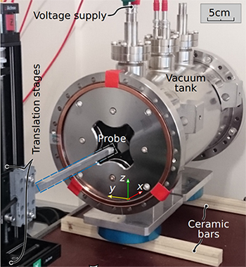
Photograph of sensor test stand using ELENA quadrupole. (Wilfried Hortshitz, Danube University Krems)
For these measurements, an electrostic quadrupole of the low energy antiproton ring ELENA at CERN was provided by their designers, Wolfgang Bartmann and Jan Borburgh from CERN. Initial measurements in October 2018 confirmed the capability of the MEMS sensor to work as an “electrostatic Hall probe”. A full quadrupole dublet was next shipped to Vienna for more detailed measurements and a full characterization of the sensor.
The findings of the group have just been published in Physical Review Letters. The authors show that the sensor can be used for detailed measurements of 3D electrostatic fields with very high precision. This gives access to a full characterization of these elements and entirely new opportunities to mitigate effects from e.g. manufacturing tolerances or misplacements. This is expected to help improve beam quality and also enhance experimental output.
More details can be found in the paper:
A. Kainz, et al., Noninvasive 3D Field Mapping of Complex Static Electric Fields, Phys. Rev. Lett. 122, 244801 (2019).